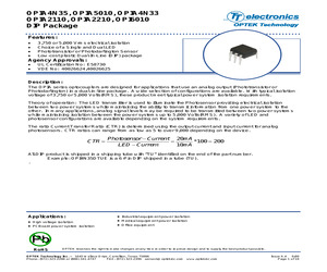
4N35, OPIA5010, OPIA4N33 OPIA2110, OPIA2210, OPI6010 DIP Package Features: * * * * 3,750 or 5,000 Vrms electrical isolation Choice of a Single and Dual LED Phototransistor or Photodarlington Sensor Low-cost plastic Dual-In-Line (DIP) package Agency Approvals: * * UL Certification No: E58730 VDE No: 40026624,40026625 Description: The OPIA series optocouplers are designed for applications that use an analog output (Phototransistor or Photodarlington) in a dual-in-line package. A wide selection of configurations are available. With typical isolation voltage of 3,750 or 5,000 Volts(RMS), these product meet typical power system isolation requirements. Theory of operation: The LED transmitter is used to illuminate the Photosensor providing electrical isolation between two power systems while maintaining the ability to transmit information from one power system to the other. In many applications, analog signal levels may be required to be transmitted between two power systems while maintaining isolation
 19 Pages, 1971 KB, Original
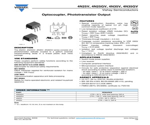
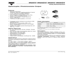
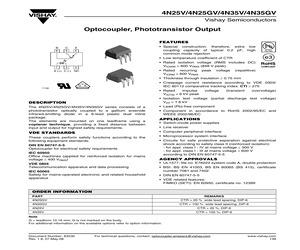
4N35V/ 4N35GV Vishay Semiconductors Optocoupler, Phototransistor Output Features * Special construction: Therefore, extra low coupling capacity of typical 0.2 pF, high Common Mode Rejection * Low temperature coefficient of CTR * Rated isolation voltage (RMS includes DC) VIOWM = 600 VRMS (848 V peak) * Rated recurring peak voltage (repetitive) VIORM = 600 VRMS * Thickness through insulation 0.75 mm B 6 C 5 E 4 1 2 3 A (+) C (-) nc V D E 17186 e3 Pb Pb-free * Creepage current resistance according to VDE 0303/IEC 60112 Comparative Tracking Index: CTI 275 * Rated impulse voltage (transient overvoltage) VIOTM = 6 kV peak * Isolation test voltage (partial discharge test voltage) Vpd = 1.6 kV * Lead-free component * Component in accordance to RoHS 2002/95/EC and WEEE 2002/96/EC Order Information Agency Approvals Description * UL1577, File No. E76222 System Code A, Double Protection * BSI: BS EN 41003, BS EN 60095 (BS415), Certificate number 7081 and 7402 * DIN EN 60747-5-2 (VDE0884) DIN EN
 10 Pages, 184 KB, Original
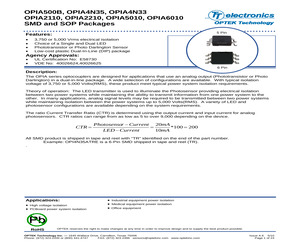
4N35, OPIA4N33 OPIA2110, OPIA2210, OPIA5010, OPIA6010 SMD and SOP Packages 5 Pin Features: * * * * 3,750 or 5,000 Vrms electrical isolation Choice of a Single and Dual LED Phototransistor or Photo Darlington Sensor Low-cost plastic Dual-In-Line (DIP) package Agency Approvals: * * UL Certification No: E58730 VDE No: 40026624,40026625 6 Pin Description: The OPIA series optocouplers are designed for applications that use an analog output (Phototransistor or Photo Darlington) in a dual-in-line package. A wide selection of configurations are available. With typical isolation voltage of 3,750 or 5,000 Volts(RMS), these product meet typical power system isolation requirements. Theory of operation: The LED transmitter is used to illuminate the Photosensor providing electrical isolation between two power systems while maintaining the ability to transmit information from one power system to the other. In many applications, analog signal levels may be required to be transmitted between two power systems whi
 23 Pages, 2041 KB, Original
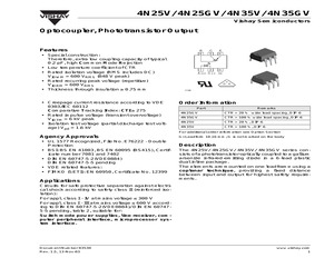
4N35V, 4N35GV Vishay Semiconductors Optocoupler, Phototransistor Output FEATURES B 6 C 5 E 4 * Special construction: therefore, extra low coupling capacity of typical 0.2 pF, high common mode rejection * Low temperature coefficient of CTR 1 2 3 A (+) C (-) NC V D E 18537_4 17201_4 * Rated isolation voltage (RMS includes DC) VIOWM = 600 VRMS (848 V peak) * Rated recurring peak VIORM = 600 VRMS The 4N25V, 4N25GV, 4N35V, 4N35GV series consists of a phototransistor optically coupled to a gallium arsenide infrared-emitting diode in a 6-lead plastic dual inline package. (repetitive) * Thickness through insulation 0.4 mm * Creepage current resistance according to VDE 0303/ IEC 60112 comparative tracking index: CTI 275 * Rated impulse VIOTM = 6 kV peak DESCRIPTION voltage voltage (transient overvoltage) * Isolation test voltage (partial discharge test voltage) Vpd = 1.6 kV * Compliant to RoHS directive 2002/95/EC accordance to WEEE 2002/96/EC and in APPLICATIONS VDE
 8 Pages, 142 KB, Original
4N35V/ 4N35GV Vishay Semiconductors Optocoupler, Phototransistor Output Features * Special construction: Therefore, extra low coupling capacity of typical 0.2 pF, high Common Mode Rejection * Low temperature coefficient of CTR * Rated isolation voltage (RMS includes DC) VIOWM = 600 VRMS (848 V peak) * Rated recurring peak voltage (repetitive) VIORM = 600 VRMS * Thickness through insulation 0.75 mm B 6 C 5 E 4 1 2 3 A (+) C (-) nc V D E 17186 e3 Pb Pb-free * Creepage current resistance according to VDE 0303/IEC 60112 Comparative Tracking Index: CTI 275 * Rated impulse voltage (transient overvoltage) VIOTM = 6 kV peak * Isolation test voltage (partial discharge test voltage) Vpd = 1.6 kV * Lead-free component * Component in accordance to RoHS 2002/95/EC and WEEE 2002/96/EC Order Information Agency Approvals Description * UL1577, File No. E76222 System Code A, Double Protection * BSI: BS EN 41003, BS EN 60095 (BS415), Certificate number 7081 and 7402 * DIN EN 60747-5-2 (VDE0884) DIN EN
 11 Pages, 215 KB, Original
4N35V/ 4N35GV Vishay Semiconductors Optocoupler, Phototransistor Output Features * Special construction: Therefore, extra low coupling capacity of typical 0.2 pF, high Common Mode Rejection * Low temperature coefficient of CTR * Rated isolation voltage (RMS includes DC) VIOWM = 600 VRMS (848 V peak) * Rated recurring peak voltage (repetitive) VIORM = 600 VRMS * Thickness through insulation 0.75 mm * Creepage current resistance according to VDE 0303/IEC 60112 Comparative Tracking Index: CTI 275 * Rated impulse voltage (transient overvoltage) VIOTM = 6 kV peak * Isolation test voltage (partial discharge test voltage) Vpd = 1.6 kV Agency Approvals * UL 1577 Recognized, File No. E76222 - Double Protection * BSI: BS EN 41003, BS EN 60095 (BS415), Certificate number 7081 and 7402 * DIN EN 60747-5-2(VDE0884) DIN EN 60747-5-5 pending * VDE related features: * FIMKO (SETI): EN 60950, Certificate No. 12399 Applications B 6 C 5 E 4 1 2 3 A (+) C (-) nc V D E 17186 Order Information Part Remarks
 10 Pages, 185 KB, Original
4N35 H11A4 4N36 H11A5 SCHEMATIC 6 1 4N28 H11A3 1 6 2 5 6 3 NC 4 1 PIN 1. ANODE 2. CATHODE 3. NO CONNECTION 4. EMITTER 5. COLLECTOR 6. BASE 6 1 BLACK PACKAGE (NO -M SUFFIX) 6 1 6 1 6 1 DESCRIPTION The general purpose optocouplers consist of a gallium arsenide infrared emitting diode driving a silicon phototransistor in a 6-pin dual in-line package. FEATURES * UL recognized (File # E90700) * VDE recognized (File # 94766) - Add option V for white package (e.g., 4N25V-M) - Add option 300 for black package (e.g., 4N25.300) * Also available in white package by specifying -M suffix, eg. 4N25-M APPLICATIONS * Power supply regulators * Digital logic inputs * Microprocessor inputs (c) 2002 Fairchild Semiconductor Corporation Page 1 of 13 5/28/02 GENERAL PURPOSE 6-PIN PHOTOTRANSISTOR OPTOCOUPLERS 4N25 4N37 4N26 H11A1 4N27 H11A2 4N28 H11A3 4N35 H11A4 4N36 H11A5 ABSOLUTE MAXIMUM RATINGS (TA = 25C unless otherwise specified) Parameter Symbol Value Units Storage Temperature TSTG -55 to +150 C Opera
 34 Pages, 470 KB, Original
4N35V, 4N35GV Vishay Semiconductors Optocoupler, Phototransistor Output FEATURES B 6 C 5 E 4 * Special construction: therefore, extra low coupling capacity of typical 0.2 pF, high common mode rejection * Low temperature coefficient of CTR 1 2 3 A (+) C (-) NC V D E 18537_4 17201_4 * Rated isolation voltage (RMS includes DC) VIOWM = 600 VRMS (848 V peak) * Rated recurring peak VIORM = 600 VRMS The 4N25V, 4N25GV, 4N35V, 4N35GV series consists of a phototransistor optically coupled to a gallium arsenide infrared-emitting diode in a 6-lead plastic dual inline package. (repetitive) * Thickness through insulation 0.4 mm * Creepage current resistance according to VDE 0303/ IEC 60112 comparative tracking index: CTI 275 * Rated impulse VIOTM = 6 kV peak DESCRIPTION voltage voltage (transient overvoltage) * Isolation test voltage (partial discharge test voltage) Vpd = 1.6 kV * Compliant to RoHS directive 2002/95/EC accordance to WEEE 2002/96/EC and in APPLICATIONS VDE
 8 Pages, 137 KB, Original
4N35V, 4N35GV Vishay Semiconductors Optocoupler, Phototransistor Output FEATURES B 6 C 5 E 4 * Special construction: therefore, extra low coupling capacity of typical 0.2 pF, high common mode rejection * Low temperature coefficient of CTR 1 2 3 A (+) C (-) NC V D E 18537_4 17201_4 * Rated isolation voltage (RMS includes DC) VIOWM = 600 VRMS (848 V peak) * Rated recurring peak VIORM = 600 VRMS The 4N25V, 4N25GV, 4N35V, 4N35GV series consists of a phototransistor optically coupled to a gallium arsenide infrared-emitting diode in a 6-lead plastic dual inline package. (repetitive) * Thickness through insulation 0.4 mm * Creepage current resistance according to VDE 0303/ IEC 60112 comparative tracking index: CTI 275 * Rated impulse VIOTM = 6 kV peak DESCRIPTION voltage voltage (transient overvoltage) * Isolation test voltage (partial discharge test voltage) Vpd = 1.6 kV * Compliant to RoHS directive 2002/95/EC accordance to WEEE 2002/96/EC and in APPLICATIONS VDE
 8 Pages, 143 KB, Original
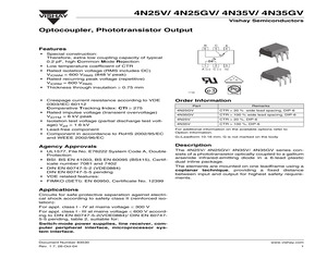
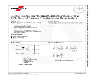
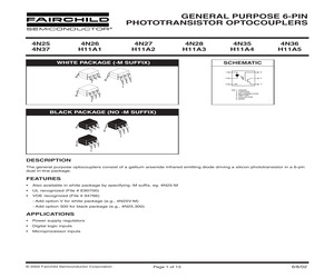
4N35M, 4N36M, 4N37M 6-Pin General Purpose Phototransistor Optocouplers Features Description Minimum Current Transfer Ratio at IF = 10 mA, The general purpose optocouplers consist of a gallium arsenide infrared emitting diode driving a silicon phototransistor in a standard plastic six-pin dual-in-line package. VCE = 10 V: - 10% for 4N27M and 4N28M - 20% for 4N25M and 4N26M - 100% for 4N35M, 4N36M and 4N37M Safety and Regulatory Approvals: - UL1577, 4,170 VACRMS for 1 Minute - DIN-EN/IEC60747-5-5, 850 V Peak Working Insulation Voltage Applications Power Supply Regulators Digital Logic Inputs Microprocessor Inputs Schematic Package Outlines 1 6 2 5 3 NC 4 PIN 1. ANODE 2. CATHODE 3. NO CONNECTION 4. EMITTER 5. COLLECTOR 6. BASE Figure 2. Package Outlines Figure 1. Schematic (c)2005 Fairchild Semiconductor Corporation 4N25M, 4N26M, 4N27M, 4N28M, 4N35M, 4N36M, 4N37M Rev. 1.3 www.fairchildsemi.com 4N25M, 4N26M, 4N27M, 4N28M, 4N35M, 4N36M, 4N37M -- 6-Pin General Pur
 13 Pages, 354 KB, Original
t over the same line as the transmitted data. In other applications the RS-232 interface handshake lines are used for modem control. R6 20K R3 3.6K V+ LM 1458 U1B + V- C12 1 F T1 MIDCOM 671-8005 R1 - T 475 1% D3, D4 4.7V ZENER C5 0.47 F 250V C4 0.033 F U2 4N35 VR1 MOV V250L20 D1 IN4004 +5V R8 22K K1 D2 IN914 R R9 10K Q1 +5 2N2222A 22K FIGURE 1: Basic Box Modem with Dual-Supply Hybrid 20 SSI 73K212AL Bell 212A/103 Single-Chip Modem data, these signals will clip if a single-ended drive approach is used. The bridged driver uses an extra opamp (U1A) to invert the signal coming from the gain setting op-amp (U1B) before sending it to the other leg of the transformer. Each op-amp then supplies half the drive signal to the transformer. The receive amplifier (U1C) picks off its signal at the junction of the impedance matching resistor and the transformer. Because the bottom leg of the transformer is being driven in one direction by U1A and the resistor is driven in the opposite direction at the same time
 1221 Pages, 5736 KB, Original
4N35V/4N35GV Vishay Semiconductors Optocoupler, Phototransistor Output FEATURES B 6 C 5 * Special construction: therefore, extra low coupling capacity of typical 0.2 pF, high common mode rejection E 4 * Low temperature coefficient of CTR 1 2 * Rated isolation voltage (RMS includes DC) VIOWM = 600 VRMS (848 V peak) 3 * Rated recurring peak VIORM = 600 VRMS A (+) C (-) NC voltage (repetitive) * Thickness through insulation 0.75 mm * Creepage current resistance according to VDE 0303/ IEC 60112 comparative tracking index: CTI 275 V D E 17186 * Rated impulse VIOTM = 6 kV peak voltage (transient overvoltage) * Isolation test voltage (partial discharge test voltage) Vpd = 1.6 kV DESCRIPTION The 4N25V/4N25GV/4N35V/4N35GV series consists of a phototransistor optically coupled to a gallium arsenide infrared-emitting diode in a 6-lead plastic dual inline package. The elements are mounted on one leadframe using a coplanar technique, providing a fixed distance between in
 10 Pages, 153 KB, Original
4N35V/ 4N35GV Vishay Semiconductors Optocoupler, Phototransistor Output Features * Special construction: Therefore, extra low coupling capacity of typical 0.2 pF, high Common Mode Rejection * Low temperature coefficient of CTR * Rated isolation voltage (RMS includes DC) VIOWM = 600 VRMS (848 V peak) * Rated recurring peak voltage (repetitive) VIORM = 600 VRMS * Thickness through insulation 0.75 mm * Creepage current resistance according to VDE 0303/IEC 60112 Comparative Tracking Index: CTI 275 * Rated impulse voltage (transient overvoltage) VIOTM = 6 kV peak * Isolation test voltage (partial discharge test voltage) Vpd = 1.6 kV B 6 C 5 E 4 1 2 3 A (+) C (-) nc V D E 17186 Order Information Part Remarks 4N25GV CTR > 20 % wide lead spacing, DIP-6 4N35GV CTR > 100 % wide lead spacing, DIP-6 4N25V CTR > 20 %, DIP-6 4N35V CTR > 100 %, DIP-6 For additional order information see Option Section Agency Approvals * UL 1577 Recognized, File No. E76222 - Double Protecti
 10 Pages, 175 KB, Original
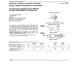
4N35, RFM4N40, RFP4N35, RFP4N40 File Number 1491 Power MOS Field-Effect Transistors N-Channel Enhancement-Mode Power Field-Effect Transistors 4 A, 350 V and 400 V ros(on): 2Q Features: SOA is power-dissipation limited Nanosecond switching speeds Linear transfer characteristics High input impedance Majority carrier device The RFM4N35 and RFM4N40 and the RFP4N35 and RFP4N40* are n-channel enhancement-mode silicon-gate power field-effect transistors designed for applications such as switching regulators, switching converters, motor driv- ers, relay drivers, and drivers for high-power bipolar switch- ing transistors requiring high speed and low gate-drive power. These types can be operated directly from inte- grated circuits. The RFM-series types are supplied in the JEDEC TO- 204AA steel package and the RFP-series types in the JEDEC TO-220AB plastic package. The RFM and RFP series were formerly RCA developmental numbers TA9393 and TA9394, respectively. MAXIMUM R
 4 Pages, 225 KB, Scan
4N35 H11A4 4N36 H11A5 SCHEMATIC 6 1 4N28 H11A3 1 6 2 5 6 3 NC 4 1 PIN 1. ANODE 2. CATHODE 3. NO CONNECTION 4. EMITTER 5. COLLECTOR 6. BASE 6 1 BLACK PACKAGE (NO -M SUFFIX) 6 1 6 1 6 1 DESCRIPTION The general purpose optocouplers consist of a gallium arsenide infrared emitting diode driving a silicon phototransistor in a 6-pin dual in-line package. FEATURES * Also available in white package by specifying -M suffix, eg. 4N25-M * UL recognized (File # E90700) * VDE recognized (File # 94766) - Add option V for white package (e.g., 4N25V-M) - Add option 300 for black package (e.g., 4N25.300) APPLICATIONS * Power supply regulators * Digital logic inputs * Microprocessor inputs (c) 2002 Fairchild Semiconductor Corporation Page 1 of 13 6/6/02 GENERAL PURPOSE 6-PIN PHOTOTRANSISTOR OPTOCOUPLERS 4N25 4N37 4N26 H11A1 4N27 H11A2 4N28 H11A3 4N35 H11A4 4N36 H11A5 ABSOLUTE MAXIMUM RATINGS (TA = 25C unless otherwise specified) Parameter Symbol Value Units Storage Temperature TSTG -55 to +150 C Operat
 31 Pages, 706 KB, Original


