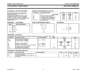
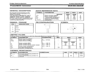
t Tj RDS(ON) BUK455 Drain-source voltage Drain current (DC) Total power dissipation Junction temperature Drain-source on-state resistance -200A 200 14 125 175 0.23 -200B 200 13 125 175 0.28 V A W C PIN CONFIGURATION DESCRIPTION 1 gate 2 drain 3 source tab BUK455-200A/B SYMBOL d tab g drain s 1 23 LIMITING VALUES Limiting values in accordance with the Absolute Maximum System (IEC 134) SYMBOL PARAMETER CONDITIONS MIN. MAX. UNIT VDS VDGR VGS Drain-source voltage Drain-gate voltage Gate-source voltage RGS = 20 k - - 200 200 30 V V V ID ID IDM Drain current (DC) Drain current (DC) Drain current (pulse peak value) Tmb = 25 C Tmb = 100 C Tmb = 25 C - Ptot Tstg Tj Total power dissipation Storage temperature Junction Temperature Tmb = 25 C - - 55 - -200A 14 10 56 -200B 13 9 52 A A A 125 175 175 W C C THERMAL RESISTANCES SYMBOL PARAMETER Rth j-mb Thermal resistance junction to mounting base Thermal resistance junction to ambient Rth j-a April 1993 CONDITIONS 1 MIN. TYP. MAX. UNIT - - 1.2 K/W - 60 - K/W Rev
 7 Pages, 43 KB, Original
 Tj RDS(ON) BUK455 Drain-source voltage Drain current (DC) Total power dissipation Junction temperature Drain-source on-state resistance; -200A 200 14 125 175 0.23 -200B 200 13 125 175 0.28 V A W C PIN CONFIGURATION DESCRIPTION 1 gate 2 drain 3 source tab BUK455-200A/B SYMBOL d tab g drain s 1 23 LIMITING VALUES Limiting values in accordance with the Absolute Maximum System (IEC 134) SYMBOL PARAMETER CONDITIONS MIN. MAX. UNIT VDS VDGR VGS Drain-source voltage Drain-gate voltage Gate-source voltage RGS = 20 k - - 200 200 30 V V V ID ID IDM Drain current (DC) Drain current (DC) Drain current (pulse peak value) Tmb = 25 C Tmb = 100 C Tmb = 25 C - Ptot Tstg Tj Total power dissipation Storage temperature Junction Temperature Tmb = 25 C - - 55 - -200A 14 10 56 -200B 13 9 52 A A A 125 175 175 W C C THERMAL RESISTANCES SYMBOL PARAMETER Rth j-mb Thermal resistance junction to mounting base Thermal resistance junction to ambient Rth j-a August 1996 CONDITIONS 1 MIN. TYP. MAX. UNIT - - 1.2 K/W - 60 - K/W Re
 7 Pages, 53 KB, Original
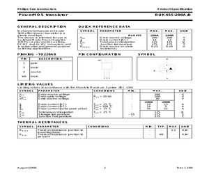
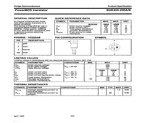
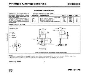
BUK455-200A/B a GENERAL DESCRIPTION QUICK REFERENCE DATA N-channel enhancement mode SYMBOL | PARAMETER MAX. | MAX. | UNIT field-effect power transistor in a plastic envelope. BUK455 -200A | -200B The device is intended for use in Vos Drain-source voltage 200 200 Vv Switched Mode Power Supplies Ip Drain current (DC) 14 13 A (SMPS), motor control, welding, Pia Total power dissipation 125 125 W DC/DC and AC/DC converters, and T Junction temperature 175 175 Cc in general purpose switching Fosom Drain-source on-state 0.23 0.28 Q applications. resistance PINNING - TO220AB PIN CONFIGURATION SYMBOL PIN DESCRIPTION | d tab > CG 1 Igate =~ , | | hh 2 {drain _! i | ie x ; tp 3 |source 1 " 9 SHY fy ; tab |drain - | | 123 s LIMITING VALUES Limiting values in accordance with the Absolute Maximum System (IEC 134) SYMBOL |PARAMETER CONDITIONS MIN. MAX. UNIT Vos Drain-source voltage - - 200 Vv Vocr Drain-gate voltage Ras = 20 kQ - 200 Vv Ves Gate-source voltage - - 30 Vv -200A -200B lo Drain current (DC Tr = 25C
 5 Pages, 242 KB, Scan
BUK455-200A/B Dn GENERAL DESCRIPTION QUICK REFERENCE DATA N-channel enhancement mode SYMBOL | PARAMETER MAX. MAX. UNIT field-effect power transistor in a plastic envelope. BUK455 -200A | -200B The device is intended for use in Vos Drain-source voltage 200 200 Vv Switched Mode Power Supplies Ip Drain current (DC) 14 13 A (SMPS), motor control, welding, Prot Total power dissipation 125 125 WwW DC/DC and AC/DC converters, and i Junction temperature 175 175 C in automotive and general purpose Rosion Drain-source on-state 0.23 0.28 Q switching applications. resistance; PINNING - TO220AB PIN CONFIGURATION SYMBOL PIN DESCRIPTION wh Ce J d 1 gate 2 drain f | 3 |source ) 9 N / tab |drain i 123 s LIMITING VALUES Limiting values in accordance with the Absolute Maximum System (IEC 134) SYMBOL |PARAMETER CONDITIONS MIN. MAX. UNIT Vos Drain-source voltage - - 200 Vv Voer Drain-gate voltage Res = 20 kQ - 200 Vv Ves Gate-source voltage - - 30 Vv -200A -200B lp Drain current (Be Trp = 25 C - 14 13 A Ip Drain curr
 5 Pages, 175 KB, Scan
BUK455-200A/B GENERAL DESCRIPTION QUICK REFERENCE DATA N-channel enhancement mode SYMBOL | PARAMETER MAX. MAX. UNIT field-effect power transistor in a plastic envelope. BUK455 -200A | -200B The device is intended for use in Vos Drain-source voltage 200 200 Vv Switched Mode Power Supplies lb Drain current (DC) 14 13 A (SMPS), motor control, welding, Prot Total power dissipation 125 125 Ww DC/DC and AC/DC converters, and T, Junction temperature 175 175 C in automotive and general purpose Rosiony Drain-source on-state 0.23 0.28 Q switching applications. resistance; PINNING - TO220AB PIN CONFIGURATION SYMBOL PIN DESCRIPTION or () d 1 |gate _ 7 : It a 2 {drain i i yes iI 3 |source \ i Foe! fe tab [drain | | 123 $s LIMITING VALUES Limiting values in accordance with the Absolute Maximum System (IEC 134) SYMBOL |PARAMETER CONDITIONS MIN. MAX. UNIT Vos Drain-source voltage - - 200 Vv Vocr Drain-gate voltage Reg = 20 kQ - 200 Vv Ves Gate-source voltage - - 30 Vv -200A -200B lp Drain current (DC) Tab = 25C
 5 Pages, 225 KB, Scan
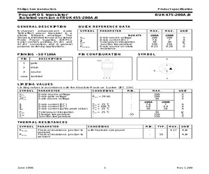
BUK455-200A/B GENERAL DESCRIPTION N-channel enhancement mode field-effect power transistor in a plastic full-pack envelope. The device is intended for use in Switched Mode Power Supplies (SMPS), motor control, welding, DC/DC and AC/DC converters, and in general purpose switching applications. PINNING - SOT186A PIN BUK475-200A/B QUICK REFERENCE DATA SYMBOL PARAMETER MAX. MAX. UNIT VDS ID Ptot Tj RDS(ON) BUK475 Drain-source voltage Drain current (DC) Total power dissipation Junction temperature Drain-source on-state resistance -200A 200 7.6 30 150 0.23 -200B 200 7 30 150 0.28 V A W C PIN CONFIGURATION SYMBOL DESCRIPTION d case 1 gate 2 drain 3 source g case isolated 1 2 3 s LIMITING VALUES Limiting values in accordance with the Absolute Maximum System (IEC 134) SYMBOL PARAMETER CONDITIONS MIN. MAX. UNIT VDS VDGR VGS Drain-source voltage Drain-gate voltage Gate-source voltage RGS = 20 k - - 200 200 30 V V V ID ID IDM Drain current (DC) Drain current (DC) Drain current (pulse peak value) Ths = 25 C T
 7 Pages, 56 KB, Original
BUK455-200A/B GENERAL DESCRIPTION QUICK REFERENCE DATA N-channel enhancement mode SYMBOL | PARAMETER MAX. | MAX. UNIT field-effect power transistor in a plastic envelope. BUK455 -200A | -200B The device is intended for use in Vos Drain-source voltage 200 200 Vv Switched Mode Power Supplies Ip Drain current (DC) 14 13 A (SMPS), motor control, welding, Poot Total power dissipation 125 125 WwW DC/DC and AC/DC converters, and T Junction temperature 176 175 Cc in general purpose switching Rosiom Drain-source on-state 0.23 0.28 2 applications. resistance PINNING - TO220AB PIN CONFIGURATION SYMBOL PIN DESCRIPTION re d 1 |gate aN ! 1 2 {drain K) 3 |source } iH g tab [drain | | | 123 s LIMITING VALUES Limiting values in accordance with the Absolute Maximum System (IEC 134) SYMBOL |PARAMETER CONDITIONS MIN. MAX. UNIT Vos Drain-source voltage - - 200 Vv Vocr Drain-gate voltage Res = 20 kQ - 200 Vv Ves Gate-source voltage - - 30 Vv -200A -200B lo Drain current be} Tb = 25 C - 14 13 A lp Drain current (DC Tp
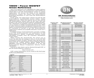
 5 Pages, 189 KB, Scan
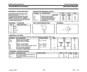
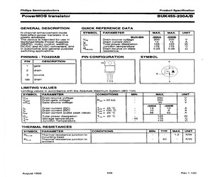
0 100 Tmb / C 120 140 160 Fig.1. Normalised power dissipation. PD% = 100PD/PD 25 C = f(Tmb) 120 1E-05 1E-03 t/s 1E-01 1E+01 Fig.4. Transient thermal impedance. Zth j-mb = f(t); parameter D = tp/T Normalised Current Derating ID% t T 0.001 1E-07 180 tp T 30 BUK455-200A ID / A 20 VGS / V = 110 6 10 100 8 7 90 80 20 70 60 5 50 10 40 30 20 4 10 0 0 0 20 40 60 80 100 Tmb / C 120 140 160 180 BUK455-200A,B ID / A ID S/ N) = 2 1.0 A 6 8 10 12 VDS / V 14 RDS(ON) / Ohm VD tp = 10 us O S( 4 16 20 4.5 4 0.8 BUK455-200A 5 5.5 6 RD 10 18 Fig.5. Typical output characteristics, Tj = 25 C. ID = f(VDS); parameter VGS Fig.2. Normalised continuous drain current. ID% = 100ID/ID 25 C = f(Tmb); conditions: VGS 10 V 100 0 100 us 0.6 1 ms DC 8 0.4 10 ms 100 ms 1 10 VGS / V = 0.2 20 0 0.1 1 10 100 VDS / V 0 1000 Fig.3. Safe operating area. Tmb = 25 C ID & IDM = f(VDS); IDM single pulse; parameter tp February 1996 4 8 12 16 ID / A 20 24 28 Fig.6. Typical on-state resistance, Tj = 25 C. RDS(ON) = f(
 7 Pages, 56 KB, Original
BUK455-200A/B ee ee ee er ee ee ee eee GENERAL DESCRIPTION QUICK REFERENCE DATA N-channel enhancement mode SYMBOL | PARAMETER MAX. MAX. UNIT field-effect power transistor in a - plastic envelope. BUK455 -200A | -200B The device is intended for use in Vos Drain-source voltage 200 200 Vv Switched Mode Power Supplies | Drain current (DC) 14 13 A (SMPS), motor control, welding, P Total power dissipation 125 1. 125 Ww DC/DC and AC/DC converters, and T Junction temperature 175 175 Cc in automotive and general purpose Psion) Drain-source on-state 0.23 0.28 Q switching applications. resistance; PINNING - TO220A8 PIN CONFIGURATION SYMBOL PIN DESCRIPTION mp O 4 1 |gate 7 2 {drain | 3 |source ) | 9 tab [drain I 123 LIMITING VALUES Limiting values in accordance with the Absolute Maximum System (IEC 134) SYMBOL | PARAMETER CONDITIONS MIN. MAX. UNIT Vos Drain-source voltage - - 200 Vv Voar Drain-gate voltage Reg = 20 kQ 200 Vv Ves Gate-source voltage - - 30 Vv -200A -200B lb Drain current (BE Tre = 25C - 14 13
 5 Pages, 285 KB, Scan
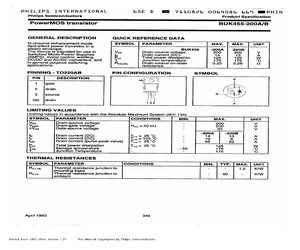
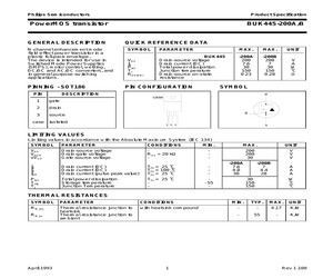
BUK455-200A BUK455-200B N-channel enhancement mode SYMBOL; PARAMETER MAX. MAX. UNIT field-effect power transistor in a plastic envelope. BUK455 | -200A | -200B The device is intended for use in Vos Drain-source voltage 200 200 Vv Switched Mode Power Supplies lo Drain current (DC) 14 13 A (SMPS), motor control, welding, Prot Total power dissipation 125 125 Ww DC/DC and AC/DC converters, T Junction temperature 175 175 c and in general purpose switching Fosiony Drain-source on-state resistance] 0.23 0.28 Q applications. MECHANICAL DATA Dimensions in mm 45 max Net Mass: 2g 10,3 13 ~ rT Pinning: O74 59 1 = Gate i min 2 = Drain i 15,8 I max 3 = Source r 35 max 5,1 not tinne max d ~f 1,3 max 4 (2x) 0.9 max (3x) Le 06 2,54 2,54 wt Me 24 9 s Fig.1 TO220AB; drain connected ta mounting base. Notes 1. Observe the general handling precautions for electrostatic-discharge sensitive devices (ESDs) to prevent damage to MOS gate oxide. 2. Accessories supplied on request: refer to Mounting instructions for TO220 en
 5 Pages, 181 KB, Scan
 conditions: VGS 10 V April 1993 1000 Fig.3. Safe operating area. Ths = 25 C ID & IDM = f(VDS); IDM single pulse; parameter tp Normalised Current Derating ID% 10 3 Rev 1.100 Philips Semiconductors Product Specification PowerMOS transistor 30 BUK445-200A/B BUK455-200A ID / A 15 20 VGS / V = gfs / S BUK455-200A 6 10 8 7 20 10 5 10 5 4 0 0 2 4 6 8 10 12 VDS / V 14 16 18 0 20 Fig.5. Typical output characteristics, Tj = 25 C. ID = f(VDS); parameter VGS 4 8 12 16 ID / A 20 24 28 Fig.8. Typical transconductance, Tj = 25 C. gfs = f(ID); conditions: VDS = 25 V BUK455-200A RDS(ON) / Ohm 1.0 0 2.4 Normalised RDS(ON) = f(Tj) a 2.2 0.8 5 4.5 4 5.5 2.0 1.8 1.6 6 0.6 1.4 1.2 8 1.0 0.8 0.4 10 VGS / V = 0.2 0.6 20 0.4 0.2 0 0 0 4 8 12 16 ID / A 20 24 28 -60 Fig.6. Typical on-state resistance, Tj = 25 C. RDS(ON) = f(ID); parameter VGS 28 ID / A -40 -20 0 20 40 60 Tj / C 80 100 120 140 Fig.9. Normalised drain-source on-state resistance. a = RDS(ON)/RDS(ON)25 C = f(Tj); ID = 7 A; VGS = 10 V
 7 Pages, 44 KB, Original
l impedance. Zth j-hs = f(t); parameter D = tp/T Fig.2. Normalised continuous drain current. ID% = 100ID/ID 25 C = f(Ths); conditions: VGS 10 V April 1993 T tp T 3 Rev 1.100 Philips Semiconductors Product Specification PowerMOS transistor 30 BUK445-200A/B BUK455-200A ID / A 15 20 VGS / V = gfs / S BUK455-200A 6 10 8 7 20 10 5 10 5 4 0 0 2 4 6 8 10 12 VDS / V 14 16 18 0 20 Fig.5. Typical output characteristics, Tj = 25 C. ID = f(VDS); parameter VGS RDS(ON) / Ohm 1.0 5 2.4 2.2 2.0 1.8 1.6 1.4 5.5 6 0.6 0.4 10 0.2 20 12 16 ID / A 20 24 28 Normalised RDS(ON) = f(Tj) a 0 0 0 4 8 12 16 ID / A 20 24 -60 -40 -20 28 Fig.6. Typical on-state resistance, Tj = 25 C. RDS(ON) = f(ID); parameter VGS 28 8 1.2 1.0 0.8 0.6 0.4 0.2 8 VGS / V = 4 Fig.8. Typical transconductance, Tj = 25 C. gfs = f(ID); conditions: VDS = 25 V BUK455-200A 4.5 4 0.8 0 ID / A 0 20 40 60 Tj / C 80 100 120 140 Fig.9. Normalised drain-source on-state resistance. a = RDS(ON)/RDS(ON)25 C = f(Tj); ID = 7 A; VGS = 10 V
 7 Pages, 55 KB, Original
553-100B BUK552-100A 435-077 100 0.28 5 10 VD MOSFET BUK552-100A BUK553-100B 353-504 100 0.31 5 1.7 VD MOSFET BUK555-100A 435-065 180 10 3 0.3 VD MOSFET BUK555-100B 353-528 200 0.2 10 17 VD MOSFET BUK456-200B BUK582-100A 434-930 200 0.23 5 10 14 VD MOSFET BUK455-200A 200 0.28 5 10 13 VD MOSFET BUK455-200B 200 12 10 0.25 Applications Key = Power Conversion = Line Switching & Protection = General Purpose Switching = Automotive = TV & Monitors = DC Motor Drive BUK582-100A BST76A VD MOSFET BST74A Technology Technology is Vertically Diffused MOSFET. 21 240V - 1000V N-CHANNEL POWERMOS TRANSISTORS VDS (V) RDS (ON) () @VGS ID (V) (max) @ 25C TECHNOLOGY (A) Cross Reference LEADED PACKAGE SOT78 (TO220AB) SOT186 TYPICAL APP. SOT54 (TO92) 240 6 10 0.3 VD MOSFET BSS89 250 7 10 0.3 VD MOSFET BSN254A 270 8 10 0.25 VD MOSFET BSN274 300 8 10 0.25 VD MOSFET BSN304 400 1 10 7.2 VD MOSFET PHP5N40 400 1.8 10 4.4 VD MOSFET PHP4N40 500 1.5 10 5.9 VD MOSFET PHP4N50 500 3 10 3.4 VD MOSFET PHP3N50 600 1.2 10 7 VD MOSFET P
 34 Pages, 410 KB, Original
45-200A BUK445-200B BUK445-400B BUK445-500B BUK445-600B BUK446-800A BUK446-800B BUK452-100A BUK452-100B BUK452-60A BUK452-60B BUK453-100A BUK453-100B BUK453-60A BUK453-60B BUK454-200A BUK454-200B BUK454-400B BUK454-500B BUK454-600B BUK454-800A BUK455-100A BUK455-200A BUK455-400B BUK455-500B BUK455-600B BUK455-60A BUK455-60B SGS-THOMSON replacement SGS-THOMSON nearest preferred IRF520 IRF530FI IRF530FI STP10NB20FP STP10NB20FP STP5NB40FP STP4NB50FP STP3NB60FP STP3NA90FI IRF540FI STP19NB20FP IRF620FI STP7NB40FP STP6NB50FP STP5NB60FP STP4NA80FI STP4NA90FI IRF520 IRF520FI STP16NE06 STP16NE06 IRF530 IRF530 STP20NE06 STP20NE06 STP10NB20 STP10NB20 STP5NB40 STP4NB50 STP3NB60 STP3NA90 IRF540 STP19NB20 STP7NB40 STP6NB50 STP5NB60 STP36NE06 STP36NE06 Industry standard BUK456-100A BUK456-100B BUK456-1000B BUK456-200A BUK456-200B BUK456-60A BUK456-60B BUK456-60H BUK456-800A BUK456-800B BUK457-400B BUK457-500B BUK457-600B BUK481-60A BUK482-100A BUK482-60A BUK517-500BE BUK543-100A BUK543-60A BUK543-60B BUK545-60A
 17 Pages, 58 KB, Original
B MTP4N40E BUK454-500B MTP4N50E FW104 MMDF2P01HDR2 BUK454-600B MTP3N60E FW201 MMDF4N01HDR2 BUK454-800A MTP4N80E FW202 MMDF4N01HDR2 BUK454-800B MTP4N80E FW203 MMDF6N03HDR2 BUK455-100A MTP27N10E FW211 MMDF4N01HDR2 BUK455-100B MTP27N10E HAT1001F MMSF4P01HDR2 BUK455-200A MTP20N20E HAT1002F MMSF7P03HDR2 BUK455-200B MTP20N20E HAT1005F MMSF7P03HDR2 BUK455-400B MTP5N40E HAT1007F MMSF3P02HDR2 BUK455-500B MTP4N50E HAT1008F MMSF3P03HDR2 BUK455-600B MTP3N60E HAT1020R MMSF7P03HDR2 BUK455-60H MTP50N06V HAT1024R MMDF2P03HDR2 BUK456-1000B MTP3N120E HAT2001F MMSF7N03HDR2 BUK456-100A MTP40N10E HAT2003F MMDF3N03HDR2 BUK456-100B MTP33N10E HAT2005F MMSF10N02ZR2 BUK456-200A MTP20N20E HAT2007F MMSF7N03HDR2 BUK456-200B MTP20N20E HAT2016R MMDF3N03HDR2 BUK456-60A MTP50N06V HAT2020R MMSF7N03HDR2 BUK456-60B MTP50N06V HAT2027 MMDF6N02HDR2 BUK456-60H MTP60N06HD IRF510 IRF510 BUK456-800A MTP4N80E IRF510A MTP10N10E BUK456-800B MTP4N80E IRF520 IRF520 BUK457-500B MTP8N50E IRF520A MTP12N10E BUK457-600B MTP6N60E IRF530 IRF530 IRF53
 8 Pages, 81 KB, Original


