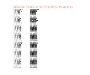
1363E CA1391E CA1394E CA1458E UPC1458C CA1458S CA1458T CA1558T CA2004 CA2111 CA2301 CA2418 CA2600 CA2603 CA2700 CA2810 CA2812 CA2818 CA2820 CA2830 CA2840 CA2850 CA2870 CA2876 CA3012 CA3014 CA3019 CA3020 CA3029 CA3039 CA3042 CA3042E CA3044 MC1741CG MC1741U MC1741G LM747 MC1747CL MC1747CL MC1747CG MC1747L MC1747L MC1747G LM748 MC1748CP1 MC1748CG MC1748U MC1748G MHW590 MHW590 MHW590 MHW590 TDA11902 TDA3190P LA1363 MC1391P UPC1394C UA1458P ECG778A MC1458CP1 MC1458G MC1558G TDA2008V MC1357 MHW1222 MHW1182 MHW1342 MHW1344 MHW1392 MHW1342 MHW593 MHW1182 MHW590 MHW592 MHW1222 MHW1182 MHW1342 MHW1221 LM3012 M5113T LM3019 CA3020A UA3029HC UA3039HC TA7051P TA7051P TA7050P HA1364 MC1390P TDA1190P MC1458P LM1458N ECG1374 LM2111 ECG726 TAA380 ECG905 ECG784 ECG908 ECG907 LA1342 A ECG704 ECG710 CA3044E CA3046 CA3052 CA3053 CA3054E CA3056 CA3059 CA3064 LA1364A CA3064E CA3064T CA3065 CA3065E LA1365N CA3066 CA3066E CA3067 CA3067E CA3068E CA3070C SN76242N CA3070E LA1369 CA3072 ECG713 CA3075E CA3076T CA3078 CA3079 CA
 314 Pages, 275 KB, Original
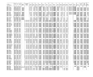
} GPK | INT 0. 2V/uS|+18V |-18V] 70C | 86dB | 6MV [SOONA 2OONA |750MWF | SMA | 12V} 15V1 30V 8SMW | 3MA | 700B | 76dB BOOK WC1741F MTU} GPK | INT 0. 3V/uS}+22V j-22V )125C | 94dB | SMV SOONA 200NA |SCOMWF| SMA | 12V] 15] 30V 7S5MW | 3MA | 700B | 760B BOOK MC1741G MTU] GPK | INT 0. 3V/uS}+22V |-22V }125C | 94dB | SMV |SOONA 2O0NA |680MWF } SMA | 12V | 15V] 30V 795MW | 3MA | 700B | 76dB BOOK MC1741L MTU] GPK | INT 0. 3V/uS1+22V j-22V }125C | 940B | SMV |SOONA 2O0NA |750MWF | SMA | 12V] 15] 30V 7S5MW | 3MA | 70dB | 76dB BOOK MC1741NCF MTU} GPK | INT 3V/uS | +18V j-18| 70C | 86dB | 6MV ISCONA ROONA |SOOMWF | SMA | 12V] 15V| 30 85MW | 3MA | 700B | 76dB BOOK MC1741NCG =| MTU} LNA| INT 0.2V/uS]+18 |-18V| 70C | 86dB | 6MV SOONA ROONA |680MNF | SMA} 12V | 15V] 30V 85MW | 3MA | 700B j 76dB BOOK MC1741NCL MTU} LNA] INT 0. 2V/uS|+18V j-18V] 70C | 86dB | 6MV SOONA OONA |750MWF } SMA | 12V | 15V) 30V 85MW | 3MA | 700B | 760B 300K MC1741NCP MTU] LNA) INT 0. 2V/uS|+18V |-18V} 70C | 86dB | 6MV SOONA POONA 625MWF
 12 Pages, 520 KB, Scan
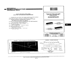
LTAGE CIRCUIT MC 1408 Series McC1508 vi Rp-2R14 fC -isv Ris = R14 Vee v Al A2 A3 Ad AB AG A? as] Vv Vo= iting ft. S248 Ae AB AS AT AB - RG) R14 2 4 8 16 32 64 128 256] Rag FIGURE 23 BIPOLAR OR INVERTED NEGATIVE OUTPUT VOLTAGE CIRCUIT MC 1408 Series mc1508 MC1741G or Equiv Yo For A = o0000000 bit configuration Vo= -Vret For a+5.0 volt output range Vref = -5.00 voits R14 = R15 = 2.5k2 ~Vret C = 37 pF (min) Ro =kQ Decrease Ro to 2.5 k for a 0 to -5.0-voit output range. This application provides somewhat lower speed, as previously discussed in the Output Voltage Range section of the General Information. MOTOROLA LINEAR/INTERFACE ICs DEVICE DATA 6-24MC1408, MC1508 APPLICATIONS INFORMATION (continued) Polarity Switching Circuit, 8-Bit Magnitude Plus Sign D-to-A Converter Bipolar outputs may also be obtained by using a polarity switch- ing circuit. The circuit of Figure 24 gives 8-bit magnitude plus asign bit. In this configuration the operational amplifier is switched between a gain of +1.0 and -1.0. A
 12 Pages, 674 KB, Scan
to +25.5 volts in 0.1-volt increments, + 0.05 volt; or 0 to 5.1 volts in 20 mV increments, +10 mV. Vret Aa 14 FIGURE 21 COMBINED OUTPUT AMPLIFIER and agolZ] VOLTAGE REFERENCE CIRCUIT a7 asold A502, MC1408 Series Aaaok] McC1S08 A304 ~ Vo A204 7 Ro 5k 108 a MC1741G R15 or Equiv Voc #8 V Co 25 pF 13 [3 16 TK 4 13 c = = ae +5 MsB Os u + Vee Rg = 2 R14 Atom Vv AI5 = R14 VEE 6 AZ azo of MC1A08 Series v Al A2 A3 Aa ABS AG A 7 as of MC1508 0 = et gfe 82, AS, BS AB, AB AT ABT Viet ey ol R14 2 4 8 16 32 64 128 256] Ry AGB OH a7oll| aa ol | tsB 1 FIGURE 23 BIPOLAR OR INVERTED NEGATIVE rh ad dr 2 | OUTPUT VOLTAGE CIRCUIT | so 16> | | Pp k | A 5 | | CV-_eeooOo! | 16k AoE | | ATA2 AZAAAS AG AT AB Ro t Lowe VEE -18 V cE Ro MC1408 Series Vo = Veep = {A MC150B o7 Yer == {a} Settling time for a 10-vatt step & 4.0 us Mer?aig Yo or Equiv For A = 00000000 bit configuration Vo* -Vret For a+5.0 volt output range = r Veet = -5.00 volts Yee sy v ~Vret C = 37 pF (min) . Ro = 5k Bipoler or Negative Output Voltage The circu
 12 Pages, 372 KB, Scan
ent to Grounded Load 7 - 0.33F These regulators can also be used as a current source when connected as above. In order to minimize dissipation the LM340-5.0 is chosen in this application. Resistor R determines the current as follows: 2 0.1F 6 + 1k 3 10k 4 MC1741G 5.0 V IO = + IQ R IQ Vout, 7.0 V to 20 V Vin - VO 2.0 V ^ 1.5 mA over line and load changes For example, a 1 A current source would require R to be a 5 , 10 W resistor and the output voltage compliance would be the input voltage less 7.0 V. The addition of an operational amplifier allows adjustment to higher or intermediate values while retaining regulation characteristics. The minimum voltage obtainable with this arrangement is 2.0 V greater than the regulator voltage. Figure 16. Current Boost Regulator Figure 17. Short Circuit Protection MJ2955 or Equiv Input RSC MJ2955 or Equiv. Input R LM340 Output 2N6049 or Equiv. R LM340 1.0F Output 0.1F 1.0F The LM340, A series can be current boosted with a PNP transistor. The MJ2955 provides curr
 2677 Pages, 35109 KB, Original
 Normally good construction techniques should be used to minimize ground loops and lead resistance drops since the regulator has no external sense lead. Figure 8. Adjustable Output Regulator Output O-] MC7805 |-O Input 7 2 => 0.33 uF 6 T 0.4 uF 3 10k 1.0k MC1741G as Vg =7.0V to 20V VIN=VQ220V The addition of an operational amplifier allows adjustment to higher or intermediate values while retaining regulation characteristics. The minimum voltage obtainable with this arrangementis 2.0 V greater than the regulator voltage. Figure 10. Short Circuit Protection MJ2955 or Equiv. RSource Rsc Input 2N6049 or Equiv. MC76XX 5 XX = 2 digits of type number indicating voltage. Output Nok The circuit of Figure 9 can be modified to provide supply protection against shortcircuits by adding a short circuit sense resistor, Age, andan additional PNP transistor. The current sensing PNP must be able to handle the short circuit current of the three-terminal regulator. Therefore, a four-ampere plastic power transistor
 15 Pages, 499 KB, Scan
 used to minimize ground loops and lead resistance drops since the regulator has no external sense lead. Figure 7. Current Regulator Figure 8. Adjustable Output Regulator MC7805 Input Output R 0.33 F IO MC7805 Input Constant Current to Grounded Load 1.0 k MC1741G VO = 7.0 V to 20 V VIN = VO 2.0 V ^ 3.2 mA over line and load changes. For example, a 1.0 A current source would require R to be a 5.0 , 10 W resistor and the output voltage compliance would be the input voltage less 7.0 V. The addition of an operational amplifier allows adjustment to higher or intermediate values while retaining regulation characteristics. The minimum voltage obtainable with this arrangement is 2.0 V greater than the regulator voltage. Figure 9. Current Boost Regulator Figure 10. Short Circuit Protection MJ2955 or Equiv. Input RSC RSource Input 0.33 F R MC78XX 1.0 F Output 1.0 F XX = 2 digits of type number indicating voltage. The MC7800 series can be current boosted with a PNP transistor. The MJ2955 provides current to
 16 Pages, 137 KB, Original
 7 0.33 F 2 0.1 F 6 3 The MC7800 regulators can also be used as a current source when connected as above. In order to minimize dissipation the MC7805C is chosen in this application. Resistor R determines the current as follows: 1.0 k I 5.0V I B O R 4 10 k MC1741G VO = 7.0 V to 20 V VIN = VO 2.0 V IB 3.2 mA over line and load changes. For example, a 1.0 A current source would require R to be a 5.0 , 10 W resistor and the output voltage compliance would be the input voltage less 7.0 V. The addition of an operational amplifier allows adjustment to higher or intermediate values while retaining regulation characteristics. The minimum voltage obtainable with this arrangement is 2.0 V greater than the regulator voltage. Figure 8. Current Regulator Figure 9. Adjustable Output Regulator RSource MJ2955 or Equiv. Input Input 0.33 F R RSC RSource MC78XX 0.33 F 2N6049 or Equiv. Output R 10 F 1.0 F MJ2955 or Equiv. 1.0 F 10 F XX = 2 digits of type number indicating voltage. MC78XX 1.0 F Output XX = 2 digits of
 28 Pages, 224 KB, Original
.33 F 2 0.1 F 6 3 The MC7800 regulators can also be used as a current source when connected as above. In order to minimize dissipation the MC7805C is chosen in this application. Resistor R determines the current as follows: 1.0 k I + 5.0V ) I B O R 4 10 k MC1741G VO = 7.0 V to 20 V VIN = VO 2.0 V IB ^ 3.2 mA over line and load changes. For example, a 1.0 A current source would require R to be a 5.0 , 10 W resistor and the output voltage compliance would be the input voltage less 7.0 V. The addition of an operational amplifier allows adjustment to higher or intermediate values while retaining regulation characteristics. The minimum voltage obtainable with this arrangement is 2.0 V greater than the regulator voltage. Figure 8. Current Regulator Figure 9. Adjustable Output Regulator RSource MJ2955 or Equiv. Input Input 0.33 F R RSC RSource MC78XX 0.33 F 2N6049 or Equiv. Output R 10 F 1.0 F MJ2955 or Equiv. 1.0 F 10 F XX = 2 digits of type number indicating voltage. MC78XX 1.0 F Output XX = 2 digits
 25 Pages, 307 KB, Original
 7 0.33 F The MC7800 regulators can also be used as a current source when connected as above. In order to minimize dissipation the MC7805C is chosen in this application. Resistor R determines the current as follows: 1.0 k I 5.0V I B O R 2 6 0.1 F 3 4 10 k MC1741G VO = 7.0 V to 20 V VIN = VO 2.0 V IB 3.2 mA over line and load changes. For example, a 1.0 A current source would require R to be a 5.0 , 10 W resistor and the output voltage compliance would be the input voltage less 7.0 V. The addition of an operational amplifier allows adjustment to higher or intermediate values while retaining regulation characteristics. The minimum voltage obtainable with this arrangement is 2.0 V greater than the regulator voltage. Figure 8. Current Regulator Figure 9. Adjustable Output Regulator RSource MJ2955 or Equiv. Input Input 0.33 F R RSC RSource 0.33 F Output MC78XX R 10 F 1.0 F 1.0 F 10 F XX = 2 digits of type number indicating voltage. MJ2955 or Equiv. 2N6049 or Equiv. MC78XX 1.0 F Output XX = 2 digits of
 20 Pages, 209 KB, Original
 7 0.33 F The MC7800 regulators can also be used as a current source when connected as above. In order to minimize dissipation the MC7805C is chosen in this application. Resistor R determines the current as follows: 1.0 k I 5.0V I B O R 2 6 0.1 F 3 4 10 k MC1741G VO = 7.0 V to 20 V VIN = VO 2.0 V IB 3.2 mA over line and load changes. For example, a 1.0 A current source would require R to be a 5.0 , 10 W resistor and the output voltage compliance would be the input voltage less 7.0 V. The addition of an operational amplifier allows adjustment to higher or intermediate values while retaining regulation characteristics. The minimum voltage obtainable with this arrangement is 2.0 V greater than the regulator voltage. Figure 8. Current Regulator Figure 9. Adjustable Output Regulator RSource MJ2955 or Equiv. Input Input 0.33 F R RSC RSource 0.33 F Output MC78XX R 10 F 1.0 F 1.0 F 10 F XX = 2 digits of type number indicating voltage. MJ2955 or Equiv. 2N6049 or Equiv. MC78XX 1.0 F Output XX = 2 digits of
 20 Pages, 206 KB, Original
 |MOTOROLA | MC4558CN MC1741CD |MOTOROLA | UA741CD MC4558BCU |MOTOROLA _ | MC4558CJ MC1741CG |MOTOROLA |UA741CH MC7805ACT |MOTOROLA |L7805ACV MC1741CP1 {MOTOROLA | UA741CN MC7805CK | MOTOROLA L7805CT MC1741CU | MOTOROLA UA741CJ MC7805CT | MOTOROLA L7805CV MC1741G MOTOROLA UA741H MC7805K MOTOROLA | L7805T MC1744U MOTOROLA UA741J MC7806ACT | MOTOROLA | L7806ACV MC1748CD | MOTOROLA UA748CD MC7806CK | MOTOROLA L7806CT MC1748BCG |MOTOROLA | UA748CH MC7806CT | MOTOROLA L7806CV MC1748CP1 |MOTOROLA | UA748CN MC7806K MOTOROLA L7806T MC1748CU | MOTOROLA UA748CJ MC7808ACT | MOTOROLA L7808ACV MC1748G MOTOROLA UA748MH MC7808CK |MOTOROLA _ | L7808CT MC1748U MOTOROLA | UA748J MC7B808CT |MOTOROLA | L7808CV MC1776CD |MOTOROLA | UA778CD MC7808K MOTOROLA | L7808T MC1776CG |MOTOROLA | UA778CH MC7812ACT |MOTOROLA | L7812ACV MC1776CP1 | MOTOROLA UA776CN MC7812CK | MOTOROLA L7812CT MC1776G MOTOROLA UA77BMH MC7812CT |MOTOROLA | L7812CV MC3302D MOTOROLA _ | MC3302D MC7812K MOTOROLA | L7812T MC3302D SIGNETICS MC3302D MC78
 11 Pages, 579 KB, Scan
33 mF 2 0.1 mF 6 3 The MC7800 regulators can also be used as a current source when connected as above. In order to minimize dissipation the MC7805C is chosen in this application. Resistor R determines the current as follows: 1.0 k 5.0V I + )I B O R 4 10 k MC1741G VO = 7.0 V to 20 V VIN = VO 2.0 V IB ^ 3.2 mA over line and load changes. For example, a 1.0 A current source would require R to be a 5.0 W, 10 W resistor and the output voltage compliance would be the input voltage less 7.0 V. The addition of an operational amplifier allows adjustment to higher or intermediate values while retaining regulation characteristics. The minimum voltage obtainable with this arrangement is 2.0 V greater than the regulator voltage. Figure 9. Current Regulator Figure 10. Adjustable Output Regulator RSource MJ2955 or Equiv. Input Input 0.33 mF R RSC RSource MC78XX 0.33 mF 2N6049 or Equiv. Output R 10 mF 1.0 mF MJ2955 or Equiv. 1.0 mF 10 mF MC78XX 1.0 mF Output XX = 2 digits of type number indicating voltage. XX =
 33 Pages, 419 KB, Original
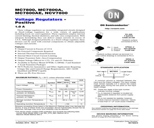
eT we Soar tae og sot me rect ORDERING INFORMATION Temperature Device Alternate Range Package MC1741CD _ OC to + 70C 80-8 MC1741CG = LM741CH, #A741HC OC to +70C Metal Carr MC1741CP1 LM741CN, pA741TC OC to +70C Plastic DIP MC1741CU - 0C to +70C Ceramic DIP MC1741G ~685C to +125C Metal Can MC1741U - ~65C to +125C Ceramic DIP MC1741 MC1741C OPERATION , .. designed for use asa summin components. No Frequency Compensation Short-Circuit Protection Low-Power Consumption No Latch Up INTERNALLY COMPENSATED, HIGH PERFORMANCE operating characteristics as a function of the external feedback Offset Voltage Null Capability Wide Common-Mode and Differential Voltage Ranges AL AMPLIFIERS g amplifier, integrator, or amplifier with OPERATIONAL AMPLIFIER SILICON MONOLITHIC INTEGRATED CIRCUIT Required G SUFFIX METAL PACKAGE CASE 601-04 Wy Offset Nult 7 84 NC the supply voitage. Note 1. For supply voltages less than +16 V, the absolute maximum input voltage is equal to EE (Top View) Pi SUFFIX MAXIMUM RATINGS (Ta = +25
 5 Pages, 354 KB, Scan


